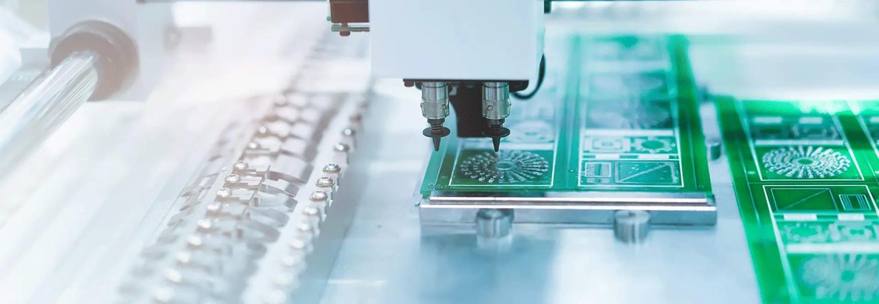
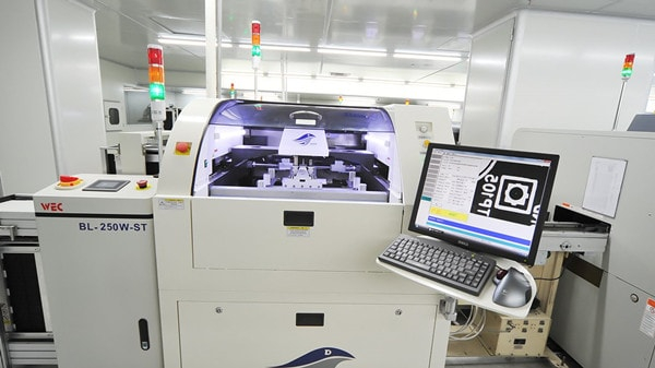
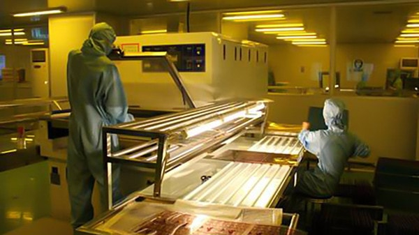
PCBA is the abbreviation of Printed Circuit Board +Assembly in English, which means that the blank PCB board goes through SMT loading, and then goes through the entire process of DIP plug-in, referred to as PCBA. This is a commonly used writing method in China, and the standard writing method in Europe and America is PCB ‘A, with “‘” added, this is called the official idiom.
Extended information:
application
3C products such as computers and related products, communication products and consumer electronics are the main application areas of PCB. According to data published by the Consumer Electronics Association (CEA), global consumer electronics sales will reach $964 billion in 2011, an increase of 10% year-on-year. The 2011 figure was pretty close to $1 trillion. CEA said that the biggest demand comes from smart phones and notebook computers, and other products that sell very well include digital cameras, LCD TVs and other products.
computer
Gartner analysts point out that notebooks have been the growth engine of the PC market over the past five years, with an average annual growth rate of nearly 40%. Based on expectations of weakening notebook computer demand, Gartner predicts that worldwide PC shipments will reach 387.8 million units in 2011 and 440.6 million units in 2012, an increase of 13.6% over 2011. In 2011, sales of removable computers, including tablets, will reach $220 billion, while desktop sales will reach $96 billion, bringing total PC sales to $316 billion, the CEA said.
The iPad 2 was officially released on March 3, 2011, and will use 4th-level Any Layer HDI in the PCB manufacturing process. The Any Layer HDI adopted by Apple’s iPhone 4 and iPad 2 will trigger a boom in the industry, and it is expected that Any Layer HDI will be applied in more and more high-end mobile phones and tablet computers in the future.
smart phone
According to the latest market research report released by Markets and Markets, the global mobile phone market size will increase to 341.4 billion US dollars in 2015, of which smartphone sales revenue will reach 258.9 billion US dollars, accounting for 76% of the total mobile phone market revenue; while Apple will Leading the global mobile phone market with a 26% market share.
iPhone 4 PCB adopts Any Layer HDI board, any layer of high-density connection board. In order to fit all the chips on the front and back sides of the iPhone 4 in a very small PCB area, using the Any Layer HDI board can avoid the waste of space caused by machine or drilling, and achieve the purpose that any layer can be turned on.
touch panel
With the popularity of iPhone and iPad all over the world and the popularity of multi-touch applications, it is predicted that the trend of touch will become the next growth driver of FPC. DisplaySearch expects 260 million touchscreen shipments for tablet PCs in 2016, up 333 percent from 2011.
e-book
According to DIGITIMES Research, global e-book shipments are expected to reach 28 million units in 2013, with a compound annual growth rate of 386% from 2008 to 2013. Analysis pointed out that by 2013, the global e-book market will reach 3 billion US dollars. The design trend of PCB boards for e-books: First, the number of layers is required to be increased; the second is to use blind buried via technology; the third is to use PCB substrates suitable for high-frequency signals.
digital camera
Digital camera production will start to stagnate in 2014 as the market becomes saturated, iSuppli said. Shipments are expected to drop by 0.6% to 135.4 million units in 2014, as low-end digital cameras will encounter strong competition from camera phones. But growth is still possible in certain areas of the industry, such as hybrid high-definition (HD) cameras, future 3D cameras, and more premium cameras such as digital single-lens reflex (DSLR). Other growth areas for digital cameras include integrating features such as GPS and Wi-Fi, increasing their appeal and potential for everyday use. Promoting the further improvement of the soft board market, in fact, the demand for soft boards is very strong for any light, thin and short electronic products.
LCD TV
Market research firm DisplaySearch expects global LCD TV shipments to reach 215 million units in 2011, an increase of 13 percent year-on-year. In 2011, LED backlight modules will gradually become mainstream due to the gradual replacement of LCD TV backlights by manufacturers. The technical trend brought to LED heat dissipation substrates: first, high heat dissipation, precision-sized heat dissipation substrates; second, strict circuit alignment Accuracy, high-quality metal circuit adhesion; 3. Use yellow light lithography to make thin-film ceramic heat dissipation substrate to improve LED high power.
LED lighting
Analysts from DIGITIMES Research pointed out that in response to the ban on production and sales of incandescent lamps in 2012, the shipments of LED bulbs will grow significantly in 2011, and the output value is estimated to be as high as about 8 billion US dollars. Driven by factors such as the implementation of subsidy policies for green products such as LED lighting, and the high willingness of stores, shops and factories to replace them with LED lighting, the global LED lighting market penetration rate has a great chance to exceed 10% in terms of output value. LED lighting, which took off in 2011, will definitely drive a large demand for aluminum substrates.