What electronics manufacturers have to know about PCBA prototyping

As an expert in the electronics manufacturing industry, you have to have a deep understanding of PCBA related knowledge, which includes manufacturing, assembly, and prototypes. In this article, we will discuss PCBA prototype manufacturing. Whether you are in automotive, consumer electronics, aerospace or any other industry, these Both will be good for you.

Special PCBA Prototyping

FPC PCBA Prototyping

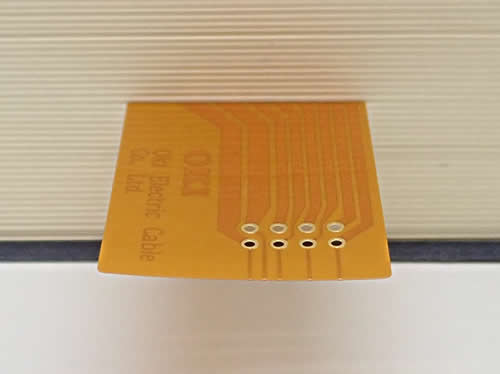
Compared to rigid PCB, FPCs are more challenging and costly to manufacture. Therefore, it is necessary to carry out prototype manufacturing to ensure that the board is functional before investing in the more expensive production process.

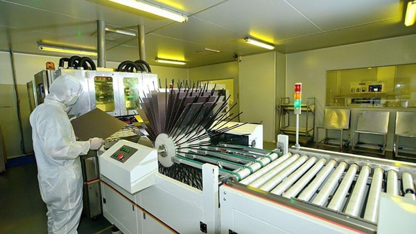
Flexible PCBA boards are composed of bendable film, copper foil, and adhesive, and they can withstand bending without damage when used in electronic products. These PCBAs are characterized by their thinness and high precision and have a multi-layer circuit structure, which makes them more difficult to produce. During PCBA prototype manufacturing, the processing plant attaches the chip to the circuit board or SMT components.

Like other substrates, electronics manufacturers are pursuing higher-level FPCBs with high voltage line density and a larger number of layers to improve PCBA performance, reduce electronic products’ size, and transmission power consumption. However, the FPCBA manufacturing process is complex, and the processing factory needs to put in more effort into prototype manufacturing. Moreover, electronic components’ application on FPC requires more attention.

Flexible PCBA (FPCBA) can be found in various electronic fields. It is an indispensable component in any high-tech product. Communication products such as smartphones use FPCB extensively. Additionally, FPCB is used in notebook computers, automotive electronics, medical, military, wearable devices, among others. As modern products become lighter, thinner, and shorter, flexible PCB importance has grown. For example, statistics show that about 20 FPCs are used in an iPhone X. FPCs also serve as antenna FPCs, backlight module FPCs, camera lens FPCs, touch screen soft boards, Touch ID soft boards, sim card soft boards, laptop screens, connecting flexible boards, automotive image sensor flexible boards, and car light unit flexible boards, illustrating the importance of flexible boards.

FS Technology uses PI, MPI, and LCP to manufacture flexible PCBA prototypes, depending on the material characteristics. MPI is Modified PI, as PIs have mostly been eliminated due to poor performance. Currently, the materials used in flexible boards are mainly MPI and LCP, with LCP offering higher performance but at a higher cost. In terms of cost-effectiveness, MPI has always been considered relatively high, with its performance improving significantly in recent years and even posing a threat to LCP. In 2018, Apple decided to replace the LCP soft board with the MPI soft board to cut expenses. The primary consideration in using these three types of flexible boards is operational attenuation. The loss of 3 does not make much difference when the frequency is low. However, as the frequency increases, PI’s loss gradually increases, and the loss of MPI and LCP also has a significant difference. Therefore, LCP’s advantage is more evident at higher frequencies. With the 5G era, some transmission frequencies will significantly increase to above 24GHz, and there will be higher quality requirements for soft boards.

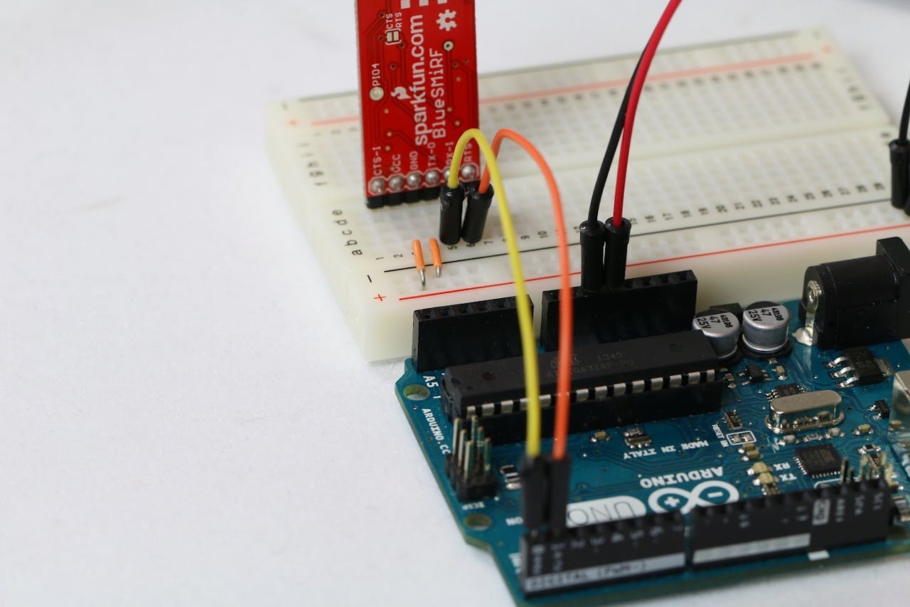
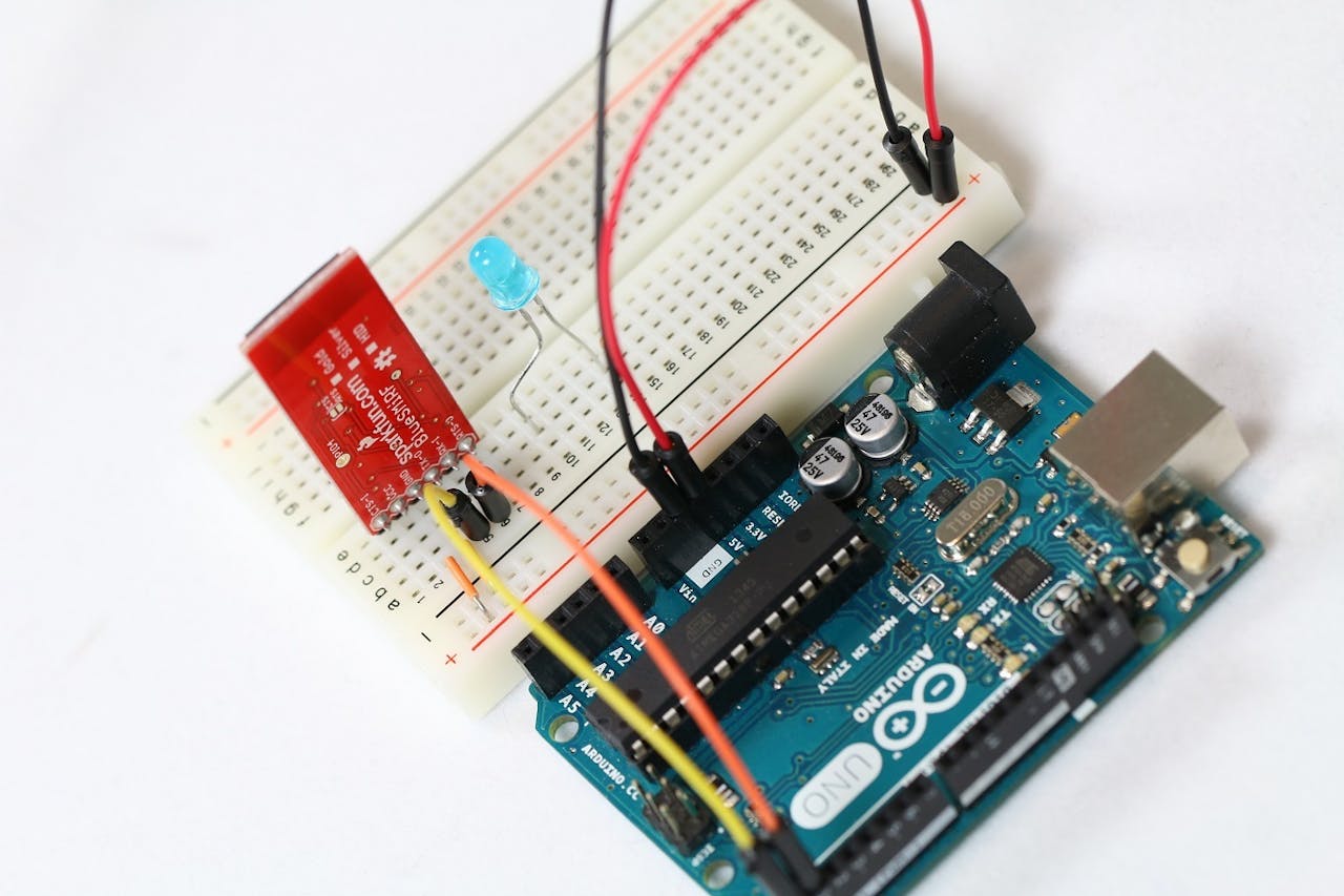
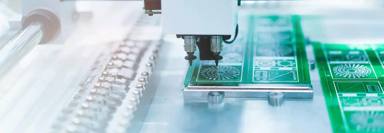
Surface treatment during PCBA prototype manufacturing

PCBA prototype Surface treatment

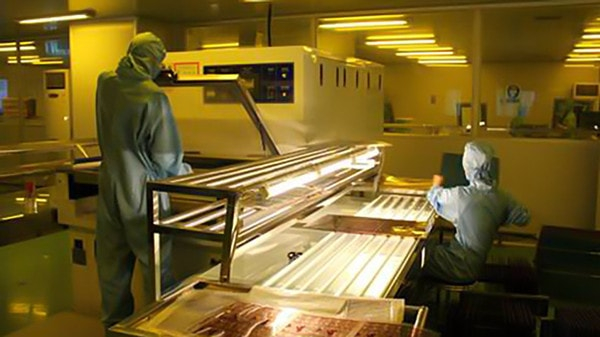
To ensure the performance and durability of a PCBA Prototyping, surface treatment is an essential step. The surface treatment helps to protect the copper surface of the PCBA from environmental factors such as humidity, oxidation, and corrosion, which can degrade the board’s performance and shorten its lifespan. The treatment also prepares the board for subsequent processes, such as soldering and component placement.

The most basic and cost-effective PCB surface treatment is the bare copper board, which is simply a board with a copper surface that has not undergone any surface treatment. This method is usually used for low-cost prototypes or in applications where the board will not be exposed to harsh environmental conditions.

The Hot Air Solder Leveling (HASL) surface treatment involves dipping the board in a molten tin-lead alloy and then leveling it with hot air. This method provides good solderability, but it has become less popular in recent years due to environmental concerns and the trend towards lead-free alternatives.

Lead-free HASL is similar to HASL but uses lead-free alloys, making it more environmentally friendly. However, this method can be more expensive than traditional HASL.

Chemical gold plating is a common surface treatment method that provides excellent protection against corrosion and oxidation. This method involves immersing the board in a gold plating solution, which deposits a thin layer of gold onto the copper surface. Gold plating is ideal for applications that require high reliability and performance, such as aerospace or military applications.

Gold plating is a more expensive surface treatment method that provides the highest level of protection against oxidation and corrosion. This method involves depositing a thicker layer of gold onto the copper surface, making it ideal for applications that require repeated use and handling.

Chemical silver is another surface treatment method that provides excellent protection against oxidation and corrosion. This method involves depositing a thin layer of silver onto the copper surface using a chemical process. Chemical silver is often used for low-cost applications where performance and reliability are not critical.

Organic Solderability Preservatives (OSP) board is a surface treatment method that uses a thin layer of organic material to protect the copper surface from oxidation and corrosion. OSP provides a flat and uniform surface that is ideal for fine pitch components, and it is often used in high-speed applications such as telecommunications or data transmission.

Key points to understand for PCBA prototyping

PCBA prototyping test

Courier service provider: Fast turnaround is essential for courier services, and FS Technology collaborates with renowned courier companies like DHL, Fedex, UPS, TNT, and EMS. Additionally, we have our own forwarder that offers lower shipping costs.

Means of transportation: Multinational trading companies can provide express, air, rail, and sea transportation based on the customer’s preferences and budget.

Popular areas: PCBA prototype manufacturing services are applicable to various industries, ensuring product quality in sectors such as semiconductors, smart homes, medical products, smart wearables, industrial control, and the Internet of Things.

Prototype manufacturing discount: Offering free prototypes is usually a misleading claim found online. However, discounts are available for high-volume products.

Choosing a prototyping company: Many prototyping companies exist in China, such as FS Technology, JCP, PCBway, among others.

Quality Control: Quality control is crucial in PCBA prototyping, and all products undergo testing before shipping to ensure they are in perfect condition.

Quotation: Typically, the quotation time for prototyping is shorter than for mass production.

PCB installation technology and steps

With the development of the electronics industry, more and more people pay attention to the “mother of electronic products” – PCBA. This FS PCBA will introduce the types of PCB assembly and the process of PCBA manufacturing for all electronics enthusiasts.

PCB Assembly Technology Types

Before starting the PCB assembly process, FS Technology will introduce you to several of the most common PCB assembly methods, which are used in the manufacture of PCBA and have unique advantages of each other:

  • SMT assembly
  • DIP assembly
  • Mixed assembly
  • BGA assembly

SMT assembly

The full name of SMT is “Surface Mount Technology”, which is the most widely used PCB assembly technology. SMT assembly uses a high-speed placement machine to quickly install SMD components on the bare PCB. The installed PCB is reflowed to cure the solder paste, and the assembly is completed after AOI inspection. With the development of miniaturization trend, electronics manufacturers rely more and more on SMT assembly. The advantages of SMT assembly include:

  • Smaller size SMD components for SMT assembly
  • For integrated circuits IC, we have SOIC, TSSOP, QFP and BGA.
  • SMT assembly allows for easy and fast automated assembly

DIP assembly

DIP assembly, also known as THT assembly, through-hole assembly, is a technology that uses through-hole technology to mount electronic components on a bare PCB. These DIP components installed on the circuit board through DIP assembly technology include leads and wires. Typical representatives of DIP components include: resistors, capacitors, inductors, PDIP ICs, transformers, transistors, IGBTs, MOSFETs, etc. The characteristics of this assembly method are as follows:

  • With the development of SMT assembly, THT technology gradually fell out and was replaced by patch technology
  • DIP assembly is mostly done by manual plug-in
  • Component size is larger
  • The process is complex and time-consuming

Mixed assembly

Hybrid assembly refers to the combination of multiple assembly technologies to complete the manufacture of PCBA boards. Usually PCBA manufacturers have both SMT and DIP capabilities. In order to realize the diversification of PCBA, these two assembly technologies are applied to one board at the same time. The workflow of the mixed assembly workshop is as follows:

  • Enter the assembly workshop through the air shower door
  • PCB bare board into the board machine
  • Transfer to solder paste printing machine by conveyor belt and perform solder paste printing
  • Then it is transported to the high-speed SMT placement machine by the conveyor belt and the placement process is completed
  • 10 Reflow soldering to solidify the solder paste
  • AOI inspection equipment inspects the PCBA that has been patched and completes the SMT assembly process
  • Manual or fully automatic DIP insert
  • After the plug-in is completed, enter the wave soldering
  • Only put into storage after multiple inspections

BGA assembly

BGA or Ball Grid Array is a type of PCB package used to mount devices such as microprocessors with hundreds of pins. It is also known as Ball Grid Array. The BGA package or IC is mounted directly onto the BGA board and soldered in place, a process known as BGA assembly.

In most cases, FS PCBA does not add solder paste but only uses solder balls when doing BGA rework. This assumes honest site preparation and a proper flux process. Solder paste is often beneficial where planarity issues may also exist.

Conditions of PCB assembly process:

Before PCB manufacturing and PCB assembly, the manufacturer must test the customer’s production data. Before assembly, the assembly company also conducts a secondary inspection of the produced bare PCB to detect whether there are PCB defects or errors that may cause failure. This process is called the design for manufacturing (DFM) process. Manufacturers must perform these basic DFM steps to ensure flawless PCBs.

Component Layout Considerations

Polarized through-hole components must be checked. The polarity of electrolytic capacitors must be checked, the polarity of diodes must be checked, and the polarity of SMT tantalum capacitors must be checked. IC notch/header orientation must be checked.

Components that require a heat sink should have enough space for other components to keep the heat sink from touching.

Hole and Via Spacing:

The hole spacing and the spacing between holes and traces should be checked. Pads and vias cannot overlap.

Copper pad, thickness, trace width should be considered.

After performing a DFM inspection, manufacturers can easily reduce manufacturing costs by reducing the number of scrapped boards. This will help with fast turnaround by avoiding failures at the DFM level. At RayPCB, we provide DFM and DFT inspections in circuit assembly and prototyping. At RayPCB, we provide PCB OEM services, wave soldering, PCB card testing and SMT assembly using state-of-the-art OEM equipment.

Windows Remote Arduino

FS PCBA project

PCB components or supplies that need to be prepared in advance

Arduino Uno Rev3

The Arduino Uno is a rigid PCB microcontroller board based on the ATmega328P (datasheet). It has 14 digital input/output pins (6 of which can be used as PWM outputs), 6 analog inputs, a 16 MHz ceramic resonator (CSTCE16M0V53-R0), a USB connection, a power jack, an ICSP header and a reset button. It includes everything needed to support the microcontroller; just connect it to a computer with a USB cable or power it with an AC-to-DC adapter or battery and you’re ready to go. You can tinker with the Uno without worrying about doing something wrong, worst case you can replace the chips for a few bucks and start over.

“Uno,” which means “Uno” in Italian, was used to mark the release of Arduino software (IDE) 1.0. The Uno board and Arduino software (IDE) version 1.0 is the reference version of the Arduino and has now evolved to newer versions. The Uno board is the first in a series of USB Arduino boards and is the reference model for the Arduino platform; see the Arduino Board Index for an exhaustive list of current, past, or obsolete boards.

Arduino Uno Rev3

SparkFun Bluetooth PCB Modem – BlueSMiRF Silver

BlueSMiRF Silver is the latest Bluetooth PCB wireless serial cable replacement! This version of the popular BlueSMiRF uses the RN-42 module, which has a somewhat smaller range than the RN-41 module used in BlueSMiRF Gold. These modems are used as serial (RX/TX) pipes. Any serial stream from 2400 to 115200bps is seamlessly passed from your computer to your target.

The remote unit can be powered from 3.3V to 6V for easy battery connection. All signal pins on the remote unit are 3V-6V tolerant. No level translation is required. Do not connect this device directly to a serial port. If you need to connect it to a computer, you will need an RS232 to TTL converter circuit.

MCL053MD

MCL053MD is a 5mm HE red circular LED PCB component with red diffuser lens, through hole mount, round lens, 15mcd luminous intensity, 625nm peak wavelength, 45° viewing angle. This LED light is made with GaAsP on GaP.

  • 85mW power consumption
  • -40 to +85°C operating temperature range
  • Multicomp Pro products are rated 4.6 out of 5 stars
  • 12 Month Limited Warranty *See terms and conditions for details
  • 96% of customers would recommend to a friend
14N9416-40.jpg (320×193)

Male/Male Jumper Wires

Manufacturer: ADAFRUIT
Manufacturer Part No: 758
Newark Part No.: 88W2570
Technical Datasheet: 758 Datasheet

88W2570-40.jpg (200×200)

RCC120610K0FKEA

MFG_RCC1206.jpg (640×640)

The start of a Windows remote Arduino PCBA project

Program the Arduino

First, let’s program the Arduino.

  • Download and install the Arduino software from the official Arduino website.
  • Connect your Arduino device to your computer using USB.
  • Start the Arduino application.
  • Verify you have the correct Arduino board selected under Tools > Boards
  • Verify you have the correct COM port selected under Tools > Ports
  • In the Arduino IDE, navigate to File > Examples > Firmata > StandardFirmata
  • Confirm that StandardFirmata will use the correct baud rate for your connection. (see note on baud rates below)
  • Press “Upload” to deploy the StandardFirmata sketch to the Arduino device.

Baud Rate

StandardFirmata communicates with Bluetooth devices using a serial line or via USB. By default it uses a baud rate of 57,600 bps. Depending on the configuration of your Bluetooth device, you may need to modify this rate. It can be found in the setup method and looks like this:

Firmata.begin(57600);

Change the value to the correct baud rate. For USB, this value is configurable in the device and Windows Remote Arduino connection parameters. If you are using a bluetooth PCBA, the baud rate depends on the device you are using.

Hardware Set Up

You can always start with a USB, WiFi or Ethernet connection, but let’s cover the simple connection of a Bluetooth PCBA device and LED, we will use the Windows Remote Arduino library to turn the LED on and off via Bluetooth!

  • Connect the power and ground rails on the rigid PCB to the 5V and GND pins on the Arduino respectively. Power connections are easily tracked using color-coded wires (red and black).
power and ground rails
  • Plug the Bluetooth device onto the rigid PCB and connect the VCC and GND pins to the power and ground rails on the rigid PCB respectively.
Plug the Bluetooth device onto the rigid PCB
  • Connect the TX-0 pin on the Bluetooth device to the RX pin on the Arduino. Likewise, connect the RX-1 pin on the Bluetooth device to the TX pin on the Arduino.
The TX-0 pin is interconnected with the Arduino's RX pin.
  • Note that the yellow wire in the picture goes from the Bluetooth device’s transmit pin to the Arduino’s receive pin, and the orange wire does the opposite. This step is critical to establishing serial communication between the Bluetooth device and the Arduino, allowing messages transmitted from one device to be received by the other.
The yellow wire is connected to the bluetooth PCB
Establish serial communication between Bluetooth device and Arduino
  • Before making this connection, make sure your code is uploaded to the Arduino. The Arduino Uno uses the same serial (TX and RX) pins to flash the device, this prevents any code being uploaded to it while another device is connected to those serial pins.
  • Add an LED to the rigid PCBA. Note that the longer (or bent) leg is the anode (positive) and the shorter leg is the cathode (negative).
Add an LED to the rigid PCBA.
  • Connect the cathode of the LED to the ground rail of the rigid PCB using a 330Ω resistor. A 330Ω resistor is striped orange, orange, brown, gold as shown.
330Ω resistor connected to rigid PCB
  • Connect the anode of the LED to any digital I/O pin on the Arduino. We use pin 13 in our example.
The anode of the LED is connected to the Arduino

Your FS PCBA setup is now ready! It should look similar to the setup shown in the image below.

FS PCBA

FS PCBA Project Code

Arduino sketching

Install Arduio Firmata Library:

Step 1.PNG (589×298)
Step 2.PNG (838×373)

Go to Sketch Menu/Include Libraries/Manage Libraries and search for “Firmata” and install the latest version of the library.

Now open and upload the “StandardFirmata” example from File/Examples/Firmata/StandardFirmata.

It is done on the Arduino side. Now we will see the application for Windows Universal Platform.

Windows Universal Platform App

Download the example repository here. If you’d rather create your own electronics PCB fabrication project, follow the project setup guide here.

Now that we’re all set, let’s get into some code!

  • Create your project

I set up a project called FS PCBA RemoteBlinky following the steps in the setup guide. In the screenshot below, you’ll see the code-behind file, MainPage.xaml.cs, which simply creates a Bluetooth connection object and passes it to the RemoteDevice class in the constructor. You’ll see that I specified my device name in this example. You can also enumerate available devices by calling the static .listAvailableDevicesAsync() function on the BluetoothSerial (and USBSerial) class before constructing the object.

project00.png (1012×657)

Notes for USB flex PCBA:

USBSerial has many options for specifying your device. In the constructor, you can provide the device’s VID and PID, just the VID, or a DeviceInformation object (obtained from the listAvailableDevicesAsync function above). Likewise, BluetoothSerial allows you to provide a device ID (as a string), a device name (also a string), or a DeviceInformation object.

You can get the VID and PID combination of a USB device by following these steps:

Open Device Manager from Control Panel or by pressing the Windows + Pause keys together and selecting the Device Manager link on the left.

  • Expand the Ports (COM and LPT) menu
  • Right click on your Arduino device and select properties
  • On the Details tab, select Hardware ID from the drop-down menu.
  • You may see multiple entries in the Value box, but any entry will have a matching PID and VID.
  • These entries have the format “USB\VID_****&PID_****”, where **** is the numeric ID value.

USBSerial usb = new USBSerial( “VID_2341”, “PID_0043” ); Guaranteed to work only with the following hardware devices:

vidpid.png (408×455)

Next, I’ll add a callback function to the RemoteDevice object’s DeviceReady event. This function is automatically called when the Bluetooth Flex PCB device is connected and all necessary settings have been initialized. You’ll notice that I haven’t implemented anything in that function at this point. Finally, call .begin() on the connection object to tell it to connect.

Flex USB PCBA code considerations:

The parameters of the .begin() function don’t matter for bluetooth flex PCBA, but you have to use the same baud rate on Arduino and UsbSerial object (first parameter). Also, the second parameter must be “SerialConfig.8N1”. The rest of the example works exactly the same no matter which connection type you use.

project01.png (1003×651)

Jump to the MainPage.xaml file and create a few buttons that turn the LEDs on and off. You’ll notice that I’ve added the button callback to the Click event and set the IsEnabled property to false, FS Tech will explain why below!

project02.png (1017×366)
  • I implemented three functions in this step. First, the OnDeviceReady function now enables the button on the UI thread! This ensures that the button is only enabled when the Bluetooth connection is ready, as this usually takes a few seconds to happen.
  • I also set up .digitalWrite() calls in the button callbacks OnButton_Click and OffButton_Click
project04.png (1141×730)

Flex PCBA Build and Deploy! Once connected, your button will be enabled and you can turn the LED on and off at will! Here’s a screenshot of this basic example running on Windows Phone 10.

screenshot.png (480×854)

I really hope you enjoy duplicating this project and using it as a baseline for an incredible new set of PCBA projects! You can quickly go from PCB to PCBA with PCB assembly to get it done in no time.

Using Flexible Rigid PCBAs to Make Electronics More Reliable

Expensive and complex discrete interconnect cables can reduce design reliability, increase design cost and overall design size. In practice, discrete interconnect cables are a disadvantageous design. For electronic product sellers it goes against the trend of miniaturization of electronic products, and for PCBA manufacturers, it is an unreliable design. For project leaders, discrete interconnect cables are not only more expensive but also more complex. Fortunately, FS Technology’s rigid-flex PCBA will be the perfect substitute.

The advantages of FS technology manufacturing rigid-flex PCB

FS Technology specializes in the production of this rigid-flex PCBA, which is designed for flexibility and reliability to provide a cost-effective and convenient solution for your electronic projects. Discrete interconnects have different conductor orientations, whereas flex PCBAs keep all conductors in a specific orientation fixed to each other. Accurate modeling and more predictable design of PCBA traces with reliability and flexibility.

In addition, in the part of the FPC, FS Technology provides gold finger contacts, allowing the edge of the FPC to be used as the male part of the connector and can be adapted to high-density designs. Today, in order to meet the needs of electronic product users, this rigid-flex PCB replaces almost all traditional discrete interconnect solutions and enables a highly modular design.

The benefits of rigid-flex PCBA for electronic projects

FS Technology’s flexible PCBA not only provides an effective method for designing and producing interconnect solutions, but also enhances the accommodation of the circuit board and becomes the focus of the solution. The use of rigid-flex PCB can make the volume of electronic products smaller, which is unmatched by traditional circuit boards. Instead of mounting components to rigid PCBs, you can mount boards produced by FS Technologies on all flexible solutions. In addition to the above advantages, the rigid part of the rigid-flex PCBA can act as a stiffener, providing your electronic project with a reliability that a flexible PCB cannot. Most of the wearable devices, digital cameras, and medical devices used today use rigid-flex PCBs instead of just FPC or rigid PCBAs.

FS Technology believes that flexible rigid PCB is the best of all flexibility solutions. Features a flex-rigid design with built-in interconnect between the two boards. Using rigid-flex PCBAs manufactured by FS Technology in different solutions, designers can accommodate 3D solutions in one assembly step. The use of rigid-flex PCBA instead of traditional circuit boards or discrete connections can shorten the assembly time of mechanical assembly. As the demand for PCBs by electronic product sellers increases, it is proved that rigid-flex PCBs are a catalyst for any electronic solution.

Although rigid-flex PCBs are better than traditional PCBs, they are very similar in the design process. As a turnkey PCB manufacturer, special attention to mechanical quality is required when creating flexible parts. When creating a 2D layout of a flexible PCB design, it is best to use a 3D modeling software to create a mockup of the flexible design, or to create a paper mockup of the design. This method is convenient for testing whether the design meets the mechanical specifications of the flexible substrate. In addition to that, the PCB you design does not need to have a bend radius smaller than what a flex PCB allows.

FS Technology recommends that you pay attention to the following points when designing rigid-flex PCBs:

  1. Increase board flexibility with staggered traces on each layer of the flex circuit.
  2. Conductors must not be routed perpendicular to the bend radius
  3. Termination areas should be reinforced with stiffeners
  4. Use a cross-hatched pattern instead of a solid plane
  5. Vias should be kept away from bend areas

Communication with turnkey rigid-flex PCB assembly company

Before sending manufacturing files of rigid-flex PCB to FS Technology, please consider the plan’s executable in advance, such as the flex board is bendable and has the highest density when nested. If a specific dimension can be achieved by bending the PCB, usually we do not bend it in the initial design, but in the assembly step. Finally, I hope you know that the few rigid-flex PCBAs you design are more expensive than flexible PCBs. Try to use a smaller number of layers for your project needs, it will be more profitable for the electronics you sell. Flexible rigid solutions should only be considered if your design has very large layer count requirements.

Finally, filling a flex PCB is very similar to filling a rigid PCB. When doing flexible PCB assembly, consider the following tips:

  1. Bake the flex PCBs for an hour, then fill them to remove any absorbed moisture.
  2. Fix the flex PCB to a hard surface to provide dimensional stability when soldered to the device.
  3. When hand-soldering the device to the flex PCB, skip the solder-intensive fixtures to avoid overheating parts of the flex PCB.

In conclusion, rigid-flex PCBs can greatly reduce the cost and complexity of your electronics manufacturing process. Rigid-flex PCBAs are an excellent alternative to traditional discrete routing solutions, offering the repeatability and reliability of PCBs in a flexible form factor. Additionally, rigid-flex PCBAs offer the opportunity to create highly complex 3D designs while maintaining low assembly costs, high levels of repeatability and reliability. In short, rigid-flex boards will allow you to handle designs that are too costly, complex or simply impossible to manufacture. Take your designs to the next level with rigid-flex boards.

Why do PCBA prototype board proofing

I believe that customers who need to purchase turnkey PCBA services know that circuit boards need to be inspected before mass production. We need to understand the product quality when we come out, and we can obtain quality assurance before PCBA prototype manufacturing. FS Technology believes that this is a necessary link, and the customer and the turnkey company discuss details and specific parameters before proceeding with production, and pass prototype testing to lay the foundation for further production. Let’s take a look at the importance of this step.

Prototype PCB bare board

Prototyping facilitates screening of manufacturers’ capabilities

A PCBA prototype can give you a clear idea of the strength of a manufacturer, especially for a manufacturer that the two parties have not worked with before. We all know that merchants must have exaggerated descriptions of goods, and the description of their own capabilities by circuit board manufacturers is the same. Therefore, we need to judge its capabilities before choosing a suitable PCBA company, rather than relying on words to understand. In order to eliminate the information difference between the manufacturer and the customer, PCBA prototype proofing provides fairness for this. You can truly understand its strength through the PCBA board samples sent by the manufacturer, so as to determine whether to establish a long-term cooperative relationship.

PCBA Prototypes Reduce Error Rates in Mass Production

The more high-quality circuit board manufacturers, the greater the processing and manufacturing pressure. A quality turnkey PCBA company must have no shortage of customers, that is, their factories are working almost 24 hours a day. A large number of orders and long work are the main reasons for PCBA defects. After all, PCBA processing needs to go through a series of complex processes. It is impossible for us to ensure that every board is correct, but we will carry out strict PCBA quality control to ensure that every process or processing step is error-free. After the circuit board has been manufactured, we can provide you with a complete PCBA function test service. FS Technology has 7 fully automatic SMT assembly equipment, and the monthly order amount received exceeds 10 million US dollars. We need to balance quality and quantity. For this reason, we suggest that customers who cooperate with FS Technology for the first time must choose to purchase prototype assembly services, which will lay the foundation for our follow-up cooperation and promote our cooperation.

Testing PCBA samples lays the groundwork for future batch processing.

The purpose of PCBA testing is to understand the performance and operational response of a new product. The functionally tested samples will lay a good foundation for future mass production. Calculation of appropriate material costs can pre-optimize quality defects, all of which must be demonstrated in advance. Efficient reference handling minimizes unexpected problems during mass production.

Prototyping PCBs prior to production is critical, as this seems to be the first step in a successful partnership with a recycler. Therefore, for protectors, one needs to select an available PCB manufacturer and provide the manufacturer with the amount or quantity of material required to process the circuit board. After the two parties communicate and negotiate, a formal PCB board inspection is required to lay a good foundation for the next step to strengthen cooperation between the two parties.

FS Technology focuses on PCBA assembly and manufacturing. In terms of PCB, we can produce single-sided, double-sided, multi-layer boards, high-precision and high-frequency high-speed PCBs, etc. The professional production technical team provides you with the guarantee of quality, delivery time and technology. In terms of quality, we share PCB component suppliers with the world’s top 500 companies; in terms of delivery, FS Technology uses the ERP system to carry out detailed production planning, and can always pay attention to the trend of each production process to ensure product delivery; Technically, our production personnel have undergone strict training and assessment to ensure product quality. Therefore, when you choose us, you will get a different service and product quality experience.

PCB Design-FS Technology

Summary: The design of the circuit board is based on the circuit diagram to perform the functions required by the circuit designer. The design of the printed circuit board is primarily a model design, which must take into account the shape of the external connectors, the correct shape of the internal electronic components, and the precise pattern of metal and hole connections. So what is the PCB design process like? FS Technology will explain the design of printed circuit boards for you

What is the design process of FS Tech PCB circuit?

1. Planning and Design

The special performance of PCB should be the main components of high-frequency components, the main components of circuits, interference components, high-voltage components, high-heating components and other components. The condition of these specific parts of the opposite sex. It must be carefully evaluated and the belt configuration must meet the operational and manufacturing requirements of the chain. Improper layout can lead to FS Technology circuit compatibility, signal integrity issues, and PCB design defects.Before you design your pcb products, you must understand the design knowledge of PCB stackup.

FS technology solder mask pcb

When designing special components, the first consideration is the size of the circuit board. Kuaiwang pointed out that when the PCB size is too large, the printing length increases, the resistance increases, the dry resistance decreases, and the cost increases; if it is too small, the heat dissipation is not good, and it is easy to interfere with adjacent pipes. After setting the FS Technology PCB dimensions, look for the location of the special features. Finally, all components in the circuit are configured according to the functionality of the device. The arrangement of special functions in a circuit board is usually done according to the following principles:

Minimize contact between high frequency components, minimize electromagnetic distribution parameters and mutual interference. Interfering elements cannot be too close to each other, and the inlet and outlet must be as far apart as possible.

2. Some components or cables may vary greatly, so their distance should be increased to avoid the risk of short circuits caused by lightning strikes. High-voltage components must be kept out of reach.

FS Tech components weighing more than 15 G can be installed and welded. Due to heat distribution, those heavy and hot components should not be placed on the board, but on the board below the main frame. Heater parts should be kept away from hot areas.

Mark point design in PCB production can solve all the above problems for you, it can avoid the risk of short circuit caused by lightning strike.

FS Technology board printed circuit

4. All panel design specifications must be considered when configuring adjustable components such as potentiometers, adjustable inductors, variable capacitors, and microswitches. Some standard switches should be used when the system allows it. Lie down and hold your hand lightly. The layout of the components must be uniform, compact and not too heavy.

For a product to be successful, it must take into account the internal quality of FS Technology. Instead, it’s important to consider the overall aesthetic, so the perfect shield will succeed.

The targeting sequence

1. Position the side assembly near power outlets, lights, switches, sockets, etc.

2. Install large-scale FS technology components, heavy components, heating components, transformers, integrated circuits and other special components.

Arrange small pieces.

3. Planning research

FS Technology hot swappable pcb

1. Is the board size and system size required to create the correct map?

2. The layout of each part is consistent, the organization is good, and the overall layout is perfect.

3. Are there levels of conflict? Sections, terms and conditions that must be published in trust may be copyrighted.

3. Common components are easy to use. Switches, Dash plug accessories, frequently replaced parts, and more.

4. Whether the distance between the heating part and the heating part is reasonable.

The PCB design program is an important course, and if you learn this, you will cut down on a lot of unnecessary time waste.

We are preparing the knowledge of Fast PCB Assembly, many people think that fast assembly and manufacturing is a measure of a company’s ability, it is not. Fast PCB Assembly
It means to complete your order within a week or a day, which is very unreliable. Although your order is completed quickly, its quality is worrying. FS Technology has always impressed customers with its high quality and first-class service awareness. I hope you will not be deceived by the Fast PCB Assembly on the advertisement.

PCB Circuit Board Design Software-FS Technology

Abstract: Design a printed circuit board based on a schematic circuit to perform the functions required by the circuit manufacturer. Print design design refers to the circuit design, which must take into account the external design of the joint, the detailed design of the internal electrical components, and the detailed design of the metal joints and holes. What are the PCB circuit board design software? FS Technology will introduce you the mainstream pbc circuit board design software

The most popular circuit board design software in China

Protel, protel 99se, protel DXP, Altium are widely used in China. All of this software is developed and continuously developed by the company; the current version, Altium Design 15, is straightforward and can be used to easily create FS Tech PCB boards. But these softwares are not suitable for making hard PCBs.

FS Technology-hot swap pcb

Design better circuit board design software

Cadence SPB software Cadence SPB is Cadence software, the latest version is Cadence SPB 16.5; ORCAD design program is a global standard, and is also the most used circuit board design software by FS Technology; PCB design and simulation are more complete, and the use is much more complicated than Protel. The requirements and features are complex; but the rules are designed for the design, so the design is better, less work, and significantly stronger than the prototype.

FS technology pcb designer

Circuit board design software that few people use

Metor Boards and EEs, which only work on BOARDSTATION UNIX systems, are not designed for PCs, so they are rarely used; the current MentorEE version is Mentor EE 7.9, Cadence SPB is the same standard as PCB design software, and in some respects is better than Cadence Poor SPB. FS Technology has hardly used this type of board design software

FS Technology pcb fabrication

The most popular circuit board design software in Europe and America

Eagle Layout is the most widely used PCB design software in Europe. Most of the PCB design software mentioned above are the most widely used, with Cadence SPB and Mentorai kings being the most ideal. If you are new to PCB design, FS Technology believes that Cadencespb is better, it can give manufacturers a good design experience and ensure good design quality.

Air conditioning PCB maintenance precautions-FS Technology

With the arrival of summer, the frequency of use of air conditioners is getting higher and higher, followed by the maintenance of air conditioners. According to statistics, 70% of air conditioners are damaged due to pcb boards. This article will explain the maintenance precautions of FS Technology’s air conditioner circuit boards.

Printed circuit board current problems

There are many problems that need to be solved in repairing an air conditioner circuit board. First, let’s explain what happens when a string is expanded. The inductance of the printed circuit is kept to a minimum because the disturbance caused by its transient current in the printed circuit of the PCB circuit is mainly inductive component. The main method is to connect a horizontal line on one side of the printed board and a vertical line on the other side, and then use a cross hole to connect the metal chemical diameter

Printed circuit board material issues

Because there will be some cross height problems between the wires of the FS Technology PCB circuit board, in order to suppress this phenomenon, when designing and wiring, try to avoid long-distance same wires, and try to separate the Is wires from each other. The signal wire should not be connected to the ground wire. It crosses the power line far in the middle, and sets up ground traces between some signal lines that are very sensitive to interference, which can effectively suppress serial interference

The actual situation of pcb maintenance

In the actual maintenance of the air conditioner computer FS Technology board, first check the power circuit reset circuit, then replace the crystal oscillator, and then check the receiving remote control circuit. Finally check for CPU replacement. Because the CPU PIN change is the most difficult and expensive, more importantly, the CPU damage is very low, do not easily replace the CPU in the microcomputer control circuit

最新文章

What electronics manufacturers have to know about PCBA prototyping

As an expert in the electronics manufacturing industry, you have to have a deep understanding of PCBA related knowledge, which includes manufacturing, assembly, and prototypes. In this article, we will discuss PCBA prototype manufacturing. Whether you are in automotive, consumer electronics, aerospace or any other industry, these Both will be good for you. Special PCBA…

PCB installation technology and steps

With the development of the electronics industry, more and more people pay attention to the “mother of electronic products” – PCBA. This FS PCBA will introduce the types of PCB assembly and the process of PCBA manufacturing for all electronics enthusiasts. PCB Assembly Technology Types Before starting the PCB assembly process, FS Technology will introduce you to…

Windows Remote Arduino

PCB components or supplies that need to be prepared in advance Arduino Uno Rev3 The Arduino Uno is a rigid PCB microcontroller board based on the ATmega328P (datasheet). It has 14 digital input/output pins (6 of which can be used as PWM outputs), 6 analog inputs, a 16 MHz ceramic resonator (CSTCE16M0V53-R0), a USB connection,…

Using Flexible Rigid PCBAs to Make Electronics More Reliable

Expensive and complex discrete interconnect cables can reduce design reliability, increase design cost and overall design size. In practice, discrete interconnect cables are a disadvantageous design. For electronic product sellers it goes against the trend of miniaturization of electronic products, and for PCBA manufacturers, it is an unreliable design. For project leaders, discrete interconnect cables…

Loading…

Something went wrong. Please refresh the page and/or try again.

PCB Design Program – FS Technology

The reason PCBs are called single-sided is because the simplest PCBs have parts on one side and wires on the other. This is because the wires only appear on one side. Multilayer boards with multiple layers of conductors require proper circuit connections between the two layers. The bridge between the chains is called a viaduct. The basic PCB design process of FS technology can be divided into four steps:

(1) FS Technology Schematic Design: Schematic design mainly uses Protel DXP schematic editor for circuit design.

Circuit Board Manufacturing and Assembly

(2) Network report generation: An online report is a report showing the circuit principle and connection relationship between different components. Bridging and connecting circuit boards and circuit board designs. With the help of the schematic network report, you can quickly find the connection between components, which is convenient for subsequent PCB design.

(3) FS Technology PCB Design: PCB design is what we usually call PCB design. This is the final converted form of the circuit diagram. The corresponding design of this part is more complicated than the schematic design. The powerful design features of Protel DXP can complement this part of the design.

(4) Generate FS Technology PCB report: After the PCB design is completed, it is necessary to generate various reports such as output report, PCB information report, network status report, etc., and finally print the PCB layout.

1. PCB classification of FS Technology

PCBs are divided into three categories: single-sided, double-sided and multi-layer printed circuit boards according to the number of layers.

1. Single-sided, the simplest PCB, the parts are concentrated on one side and the wires are concentrated on the other side. This type of PCB is called single-sided because the wires only appear on one side. Single panels are generally easy to manufacture and inexpensive, but they have the disadvantage that they cannot be used for overly complex products.

2. Both sides are extensions of one side. If single-layer wiring is not what your electronics require, use both sides. There are copper pours and traces on both sides, allowing the wires between the two layers to pass through vias to form the desired net connections.

3. FS technology multilayer board is a printed circuit board in which three or more layers of conductive patterns and insulating materials are separated by lamination and connected to each other as needed. Multilayer circuit is the product of the development of electronic information technology in the direction of high speed, multi-function, large capacity, small capacity, thinner and lighter.

Printed circuit boards are divided into flexible boards (FPC), rigid boards (PCB) and rigid flexible boards (FPCB) according to their characteristics.

2. FS Technology’s PCB inspection method

1. Nadella bed test method

The method includes connecting a source loading probe to each detection point on a printed circuit board. Is the pressure of each probe 100 connected to the spring? -? These. 200 g? To ensure good contact at each detection point, this connected probe is called a “bed of needles”. Under the control of the test software, breakpoints and test signals can be programmed, and the inspector can receive information about all breakpoints.

PCB Design

2. FS Technology PCB observation

Due to the small size and complex structure of the PCB, special observation equipment is also required to observe the PCB. Typically, portable video microscopes are used to observe the structure of printed circuit boards. Using the video microscope camera, you can clearly see the microscopic structure of the microscope circuit board. This simplifies FS Technologies PCB design and testing.

3. Dual-probe flying probe test method

The flying probe is independent of the pin pattern attached to the fixture or stand. Based on this system, two or more probes are attached to a small head that can move freely in the x-y plane, the reference point is CADI? Directly controlled by Gerber data. Dual probes can move within 4 miles of each other. The probes can move independently of each other, and there is no limit to the distance between them. The tester with two arms that can move back and forth is based on capacitance measurements. Press the PCB firmly against the metal plate insulator, which acts as the capacitor’s other metal plate. When there is a short between lines, the capacitance will be greater than the capacitance at a particular point.

最新文章

Why do PCBA prototype board proofing

I believe that customers who need to purchase turnkey PCBA services know that circuit boards need to be inspected before mass production. We need to understand the product quality when we come out, and we can obtain quality assurance before PCBA prototype manufacturing. FS Technology believes that this is a necessary link, and the customer and the…

PCB Design-FS Technology

Summary: The design of the circuit board is based on the circuit diagram to perform the functions required by the circuit designer. The design of the printed circuit board is primarily a model design, which must take into account the shape of the external connectors, the correct shape of the internal electronic components, and the…

PCB Circuit Board Design Software-FS Technology

Abstract: Design a printed circuit board based on a schematic circuit to perform the functions required by the circuit manufacturer. Print design design refers to the circuit design, which must take into account the external design of the joint, the detailed design of the internal electrical components, and the detailed design of the metal joints…

Air conditioning PCB maintenance precautions-FS Technology

With the arrival of summer, the frequency of use of air conditioners is getting higher and higher, followed by the maintenance of air conditioners. According to statistics, 70% of air conditioners are damaged due to pcb boards. This article will explain the maintenance precautions of FS Technology’s air conditioner circuit boards. Printed circuit board current…

Loading…

Something went wrong. Please refresh the page and/or try again.

ESD Suppression Stop PCB Design-FS Technology

PCB wiring is a key factor in ESD protection, FS Technology believes that a reasonable PCB design can reduce unnecessary costs caused by fault inspection and rework. In PCB design, it is more important to overcome the electromagnetic interference (EMI) electromagnetic field effect generated by the discharge current, because the transient voltage suppression stopper (TVS) diode is used to suppress the direct charge injection caused by the ESD discharge.

This article will provide optimized ESD protection for PCB design criteria.

1. Circuit loop.

When current enters circuit loops by induction, these loops are closed and have variable magnetic flux. The current range is proportional to the area of ​​the ring. Larger loops contain more magnetic flux and therefore have stronger current induction in the circuit. Therefore, the loop area must be reduced. The most common loop consists of power and ground wires.

Multilayer PCB designs employ power and ground planes, where possible. Multilayer circuit boards not only minimize the circuit area between power and ground, but also reduce the high-frequency EMI electromagnetic fields generated by ESD pulses. If multilayer boards were not possible, FS Technology would have to connect the circuits for the power and ground lines into a grid. The grid connection can play the role of power and ground, and the printed lines of each layer should pass through holes and the connection interval in each direction should be within 6 cm. In addition, when wiring, the power and ground printed lines produced by FS Technology are as close as possible, which can also reduce the loop area.

Another way to reduce loop area and induced current is to reduce parallel paths between interconnects. When a signal cable longer than 30 cm must be used, a protective wire can be used. A better approach is to place the ground near the signal lines. The signal line should be within 13mm of the protection line or grounding line. Arrange long signal wires (>30cm) or power wires and their ground wires of each sensitive element in a crossover. Crossovers must be separated from top to bottom or left to right.

pcb assembly smt

2. The length of the circuit connection.

Long signal lines can also be used as antennas for receiving ESD pulse energy. Trying to use short signal lines can reduce the efficiency of antennas receiving ESD electromagnetic fields. In order to reduce the printed line length of the interconnection, FS Technology will try to place the interconnection equipment in the adjacent position.

3. Inject the ground charge.

Direct discharge of ESD to the ground plane can damage sensitive circuits. Use one or more high frequency bypass capacitors between the power and ground of the consumables. Bypass capacitors reduce charge injection and maintain the voltage difference between the power and ground ports. The TVS shunts the induced current, maintaining the potential difference of the TVS clamping voltage. To reduce parasitic inductive effects, TVS and capacitors should be placed as close as possible to the protected IC.

最新文章

PCB Design Program – FS Technology

The reason PCBs are called single-sided is because the simplest PCBs have parts on one side and wires on the other. This is because the wires only appear on one side. Multilayer boards with multiple layers of conductors require proper circuit connections between the two layers. The bridge between the chains is called a viaduct.…

Mark point design in PCB production-FS Technology

1. The PCB must have a Mark point corresponding to the positioning of the entire board on the diagonal of the long side of the board. Chips with an IC pin center distance of less than 0.65mm on FS Technology’s circuit boards should have a Mark point corresponding to the chip positioning on the diagonal…

Optical Fiducial PCB Design-FS Technology

On a PCB with a patch, in order to locate the entire PCB, it is usually necessary to place the optical positioning points on the four corners of the PCB, generally three.Common reference points mainly include three types of board reference points, unit reference points and local reference points. 1. Reference point structure (1) Panel…

Mark point design in PCB production-FS Technology

1. The PCB must have a Mark point corresponding to the positioning of the entire board on the diagonal of the long side of the board. Chips with an IC pin center distance of less than 0.65mm on FS Technology’s circuit boards should have a Mark point corresponding to the chip positioning on the diagonal…

Loading…

Something went wrong. Please refresh the page and/or try again.

Mark point design in PCB production-FS Technology

1. The PCB must have a Mark point corresponding to the positioning of the entire board on the diagonal of the long side of the board.

Chips with an IC pin center distance of less than 0.65mm on FS Technology’s circuit boards should have a Mark point corresponding to the chip positioning on the diagonal of the long side of the IC; when there are patches on both sides of the pcb, both sides of the pcb should be Add Mark points based on this article.

2. The edge of the PCB should retain the 5mm process edge (the minimum spacing requirement for the machine to clamp the PCB).

Chips whose center-to-center distance between IC pins is less than 0.65mm should be greater than 13mm from the edge of the board (including the edge of the process); the four corners of the board should be chamfered with a φ5 arc. Judging from the current bending degree of PCB wings, the optimal splicing length is about 200mm (equipment processing size: maximum length is 330mm; maximum width is 250mm), try not to spell in the width direction to prevent bending during production.

3. MARK point functions and categories.

Mark points, also known as fiducials, provide a common measurable point for all steps in the assembly process to ensure that each assembly device can accurately locate the circuit pattern. Therefore, FS Technology believes that the Mark point is crucial for SMT production.

4. MARK point design specification recommended by our department.

1) Shape: It is recommended to mark the Mark point as a diameter: R=1.0mm solid circle;
2) Form a complete MARK point, including marked points (or feature points) and open areas.
3) Position: The Mark point is located at the relative position of the diagonal on the veneer or puzzle, and is separated as much as possible; it is best to distribute it at the longest diagonal position (such as the MARK point position diagram).
4) In order to ensure the installation accuracy requirements of FS Technology, SMT requirements: each PCB must have at least one pair of MARK points for the SMT machine to identify, and there must be a single-board MARK (when assembling).
Panel MARK or combined MARK only play a role of auxiliary positioning.
5) When assembling, the relative positions of the MARK points of each single board must be the same.
The position of the MARK point cannot be moved for any reason, resulting in asymmetrical position of the MARK point of each board;
6) All MARK points on the PCB are only valid: two MARKs appearing in pairs on the same diagonal are valid.
So MARK points must appear in pairs to be used (MARK point location map).

7) The distance between the MARK point (edge ​​of the open area) and the edge of the PCB must be ≥5.0mm (minimum spacing requirements for the machine to clamp the PCB)

8) Requirements for open areas.

Around the mark point marking, there must be an open area with no other circuit features or markings.
The radius of the circle in the open area is R≥2R, where R is the radius of the MARK point.
When R reaches 3R, the machine recognition effect is better.

9) PBC Materials

Mark point markings can be bare copper, which is protected by a transparent anti-oxidant coating. If solder mask (solder mask) is used, the mark point or its open area should not be covered.

10) PBC Contrast.

A. The best identification performance is achieved when there is a high contrast between the mark point markings and the matrix material of the printed board.
B. The internal background must be the same for all mark points.
MARK classification:
1) Mark points are used for solder paste printing and component placement optical positioning.
According to the function of Mark points on the PCB, it can be divided into panel Mark points, single-board Mark points, local Mark points (also known as device-level Mark points),
2) There should be at least three Mark points on the edge of the FS technology paneling process and the veneer that does not need paneling, distributed in an L shape, and the diagonal Mark points are asymmetrical about the center.
3) If there are mounted components on both sides, then there must be mark points on each side.
4) There should be mark points on the board that needs to be assembled as much as possible. If there is no place to place the mark point, the mark point cannot be placed on the board.
5) For QFP with lead center distance ≤ 0.5mm and BGA equipment with center distance ≤ 0.8mm, the local Mark point should be set near the diagonal of the component center point for accurate positioning.
6) If several SOP devices are relatively close (≤100 mm) to form an array, they can be regarded as a whole, and two local Mark points are designed at their diagonal positions.

最新博客

ESD Suppression Stop PCB Design-FS Technology

PCB wiring is a key factor in ESD protection, FS Technology believes that a reasonable PCB design can reduce unnecessary costs caused by fault inspection and rework. In PCB design, it is more important to overcome the electromagnetic interference (EMI) electromagnetic field effect generated by the discharge current, because the transient voltage suppression stopper (TVS)…

Designed PCB Stackup – FS Technology

Before designing a multi-layer PCB circuit board, the designers of FS Technology must first determine the circuit board structure used, that is, decide to use a 4-layer, 6-layer or more circuit board, and then according to the size and electromagnetic compatibility of the circuit board. (EMC) requirements to determine the size of the circuit board.After…

What is turnkey printed circuit board assembly

The one-stop service for PCBA circuit board assembly is the good news for customers, that is, customers package their own requirements for circuit board assembly, hand over all the materials to FS Technology, and FS Technology directly assembles the finished product and sends it to the customer, including “assembly and detection”. Customers only need to accept the…

Optical Fiducial PCB Design-FS Technology

On a PCB with a patch, in order to locate the entire PCB, it is usually necessary to place the optical positioning points on the four corners of the PCB, generally three.
Common reference points mainly include three types of board reference points, unit reference points and local reference points.

1. Reference point structure

(1) Panel datum point and unit datum point.


Shape/Size: 40mil diameter solid circle.
FS Technology Solder Mask Window: A circle concentric with the reference point, the size is twice the diameter of the reference point.
A 2mm diameter edge requires a round or octagonal copper wire as a guard ring.
The internal background of the optical positioning reference symbols on the same board should be the same, that is, whether there is copper foil under the three reference symbols should be consistent.

(2) Local datum point.

Parts such as QFP and pitch ≤0.4mm BGA, CSP, FC need to place local fiducials.
Size/Shape: Solid circle, 40mil diameter.
Solder mask opening: The size is processed according to the ordinary pad, and the outer ring copper ring cannot.

2. Place the datum point:

General principles:

The veneer for processing SMT equipment must be placed with fiducial points.
The number of single-sided reference points is greater than or equal to 3.
For single-sided layout, simply place the datum point on the component face.
..When A5I5^0L-z1m+PPCB is double-sided layout, the fiducials are placed on both sides.
For the datum points placed on both sides, except for mirror splicing, the positions of the datum points on both sides are basically the same.

(1) The reference point for FS Technology to place the puzzle.


Panel datum points and cell datum points need to be placed.
There are three panel fiducials and unit fiducials.
The edges of the board are distributed in an L shape, and keep them as far away as possible.
Figure A below shows the location requirements for the panel datum points.
When using a mirror-symmetrical panel, the reference point on the auxiliary side must meet the requirements of overlapping after flipping, as shown in Figure B below.

(2) The datum point for placing the cell board.


The number of reference points is three, distributed in an L shape on the edge of the board, and the distance between each reference point should be as far as possible.
The edge of the reference point must be greater than 5mm.
If all four edges are not guaranteed to be satisfied, the transmission edge should at least satisfy the requirements.

最新博客

What is PCBA

PCBA is the abbreviation of Printed Circuit Board +Assembly in English, which means that the blank PCB board goes through SMT loading, and then goes through the entire process of DIP plug-in, referred to as PCBA. This is a commonly used writing method in China, and the standard writing method in Europe and America is…

The use of PCBA

Regarding what PCBA does, we recommend everyone to learn about it by understanding the role of PCBA processing equipment. PCBA processing is an electronic processing industry with a relatively high degree of integration of machinery and equipment. The use of more and more mature processing machinery and equipment and the improvement of manufacturing processes have…

Mark point design in PCB production-FS Technology

1. The PCB must have a Mark point corresponding to the positioning of the entire board on the diagonal of the long side of the board.

Chips with an IC pin center distance of less than 0.65mm on FS Technology’s circuit boards should have a Mark point corresponding to the chip positioning on the diagonal of the long side of the IC; when there are patches on both sides of the pcb, both sides of the pcb should be Add Mark points based on this article.

2. The edge of the PCB should retain the 5mm process edge (the minimum spacing requirement for the machine to clamp the PCB).

Chips whose center-to-center distance between IC pins is less than 0.65mm should be greater than 13mm from the edge of the board (including the edge of the process); the four corners of the board should be chamfered with a φ5 arc. Judging from the current bending degree of PCB wings, the optimal splicing length is about 200mm (equipment processing size: maximum length is 330mm; maximum width is 250mm), try not to spell in the width direction to prevent bending during production.

3. MARK point functions and categories.

Mark points, also known as fiducials, provide a common measurable point for all steps in the assembly process to ensure that each assembly device can accurately locate the circuit pattern. Therefore, FS Technology believes that the Mark point is crucial for SMT production.

4. MARK point design specification recommended by our department.

1) Shape: It is recommended to mark the Mark point as a diameter: R=1.0mm solid circle;
2) Form a complete MARK point, including marked points (or feature points) and open areas.
3) Position: The Mark point is located at the relative position of the diagonal on the veneer or puzzle, and is separated as much as possible; it is best to distribute it at the longest diagonal position (such as the MARK point position diagram).
4) In order to ensure the installation accuracy requirements of FS Technology, SMT requirements: each PCB must have at least one pair of MARK points for the SMT machine to identify, and there must be a single-board MARK (when assembling).
Panel MARK or combined MARK only play a role of auxiliary positioning.
5) When assembling, the relative positions of the MARK points of each single board must be the same.
The position of the MARK point cannot be moved for any reason, resulting in asymmetrical position of the MARK point of each board;
6) All MARK points on the PCB are only valid: two MARKs appearing in pairs on the same diagonal are valid.
So MARK points must appear in pairs to be used (MARK point location map).

7) The distance between the MARK point (edge ​​of the open area) and the edge of the PCB must be ≥5.0mm (minimum spacing requirements for the machine to clamp the PCB)

8) Requirements for open areas.

Around the mark point marking, there must be an open area with no other circuit features or markings.
The radius of the circle in the open area is R≥2R, where R is the radius of the MARK point.
When R reaches 3R, the machine recognition effect is better.

9) PBC Materials

Mark point markings can be bare copper, which is protected by a transparent anti-oxidant coating. If solder mask (solder mask) is used, the mark point or its open area should not be covered.

10) PBC Contrast.

A. The best identification performance is achieved when there is a high contrast between the mark point markings and the matrix material of the printed board.
B. The internal background must be the same for all mark points.
MARK classification:
1) Mark points are used for solder paste printing and component placement optical positioning.
According to the function of Mark points on the PCB, it can be divided into panel Mark points, single-board Mark points, local Mark points (also known as device-level Mark points),
2) There should be at least three Mark points on the edge of the FS technology paneling process and the veneer that does not need paneling, distributed in an L shape, and the diagonal Mark points are asymmetrical about the center.
3) If there are mounted components on both sides, then there must be mark points on each side.
4) There should be mark points on the board that needs to be assembled as much as possible. If there is no place to place the mark point, the mark point cannot be placed on the board.
5) For QFP with lead center distance ≤ 0.5mm and BGA equipment with center distance ≤ 0.8mm, the local Mark point should be set near the diagonal of the component center point for accurate positioning.
6) If several SOP devices are relatively close (≤100 mm) to form an array, they can be regarded as a whole, and two local Mark points are designed at their diagonal positions.

Designed PCB Stackup – FS Technology

Before designing a multi-layer PCB circuit board, the designers of FS Technology must first determine the circuit board structure used, that is, decide to use a 4-layer, 6-layer or more circuit board, and then according to the size and electromagnetic compatibility of the circuit board. (EMC) requirements to determine the size of the circuit board.
After determining the number of layers, determine where to place the internal electrical layers and how to distribute the different signals on these layers. This is the choice of the multilayer PCB stack-up structure.
Laminated structure is not only an important factor affecting the EMC performance of PCB boards, but also an important means to suppress electromagnetic interference.
This section will introduce the related content of the multi-layer PCB board stack-up structure of FS Technology.
After each PCB engineer counts the number of layers, each PCB engineer cannot avoid the relative arrangement between them;

1. More factors need to be considered to determine the laminate structure of the multi-layer PCB board.
In terms of wiring, the more layers, the better for wiring, but the cost and difficulty of manufacturing the board will also increase.
For FS Technology PCB manufacturers, the symmetry of the laminated structure is the focus of attention in the PCB manufacturing process, so the selection of the number of layers needs to consider the needs of various aspects to achieve the best balance. For experienced designers, after completing the pre-layout of components, the analysis will focus on the wiring bottlenecks of FS Technology’s PCBs. Combine other EDA tools to analyze the wiring density of the circuit board; then integrate the signal lines with special wiring requirements, such as differential lines, the number and type of sensitive signal lines, to determine the number of signal layers; then determine the internal electrical layers according to the type of power supply quantity. isolation and anti-interference requirements. In this way, the board count of the entire circuit board is basically determined.

2. The ground below the component surface (the second layer) provides the equipment shielding layer and reference plane for the top layer wiring;
The sensitive signal layer should be adjacent to the inner power layer (internal power layer/ground layer), and the large copper film of the inner power layer is used to shield the signal layer. The high-speed signal transmission layer in the circuit should be a signal intermediate layer, sandwiched between two internal power supply layers. In this way, the copper films of the two inner electrical layers can provide electromagnetic shielding for high-speed signal transmission, and FS Technology can effectively limit the radiation of high-speed signals between the two inner electrical layers at the same time, without causing external interference.

fs tech

3. All signal layers as close as possible to the ground plane;

4. Try to avoid two signal layers directly adjacent to each other; crosstalk is easily introduced between adjacent signal layers, resulting in circuit failure.
Effectively avoid crosstalk by adding a ground plane between the two signal layers.

5. The main power supply should be as adjacent as possible;

5. The symmetry of the laminate structure.

6. For the layer layout of the motherboard, it is difficult to control the parallel long-distance wiring of the existing motherboard.
For the board-level operating frequency above 50MHZ (refer to the operating frequency below 50MHZ and relax it appropriately), FS Technology recommends the arrangement principles:
Component surface. The welding surface is a complete ground plane (shielding);
No adjacent parallel wiring layers;
All signal layers as close as possible to the ground plane;
Critical signals are adjacent to the formation and do not cross the segmented area.

Note: When setting the layers of a specific PCB, the above principles should be flexibly grasped. On the basis of understanding the above principles, according to the needs of the actual single board, such as: whether a key wiring layer, power supply, and ground plane division are required, etc. , to determine the arrangement of the layers, do not rigor or hold on to it.

7. Multiple grounded inner electrical layers can effectively reduce the grounding impedance. For example, the A signal layer and the B signal layer use separate ground planes, which can effectively reduce common mode interference.

FS Technology – the best circuit board manufacturer in the world

最新文章

What is turnkey printed circuit board assembly

The one-stop service for PCBA circuit board assembly is the good news for customers, that is, customers package their own requirements for circuit board assembly, hand over all the materials to FS Technology, and FS Technology directly assembles the finished product and sends it to the customer, including “assembly and detection”. Customers only need to accept the goods after receiving the goods.

What exactly does FS Technology’s one-stop service include?

FS Technology’s one-stop PCBA assembly service includes PCB design, PCB proofing, PCBA processing (including SMT, DIP), connector crimping, BGA soldering, rework, reballing, PCBA testing,turnkey printed circuit board assembly, packaging and delivery.

FS Technology is customer-centric and thinks about PCBA services from the perspective of customers. Customers only need to put forward requirements, solutions and final product sales. It is the principle of FS Technology to let customers devote themselves to the research and development and sales of new products, and save a lot of time, energy and production costs for customers.

Different from traditional circuit board manufacturing

According to the traditional method, due to the insufficient ability of electronic product manufacturers, they often find professional PCB manufacturers to make circuit boards, and DIP or SMT manufacturers to make patches, and finally assemble, test and sell the products themselves after acceptance. This traditional approach will cost customers more money and time.

FS Technology’s circuit board assembly service provides customers with a total PCBA manufacturing solution service. We can shorten production cycles while reducing overhead. Through PCB circuit board manufacturing, SMT processing, electronic component procurement and other processes, the comprehensive cost of personnel, warehousing, logistics, etc. is truly reduced, and the risks and cycles of the supply chain are greatly shortened and reduced.

最新文章

What is PCBA

PCBA is the abbreviation of Printed Circuit Board +Assembly in English, which means that the blank PCB board goes through SMT loading, and then goes through the entire process of DIP plug-in, referred to as PCBA. This is a commonly used writing method in China, and the standard writing method in Europe and America is PCB ‘A, with “‘” added, this is called the official idiom.

Extended information:

application

3C products such as computers and related products, communication products and consumer electronics are the main application areas of PCB. According to data published by the Consumer Electronics Association (CEA), global consumer electronics sales will reach $964 billion in 2011, an increase of 10% year-on-year. The 2011 figure was pretty close to $1 trillion. CEA said that the biggest demand comes from smart phones and notebook computers, and other products that sell very well include digital cameras, LCD TVs and other products.

computer

Gartner analysts point out that notebooks have been the growth engine of the PC market over the past five years, with an average annual growth rate of nearly 40%. Based on expectations of weakening notebook computer demand, Gartner predicts that worldwide PC shipments will reach 387.8 million units in 2011 and 440.6 million units in 2012, an increase of 13.6% over 2011. In 2011, sales of removable computers, including tablets, will reach $220 billion, while desktop sales will reach $96 billion, bringing total PC sales to $316 billion, the CEA said.

The iPad 2 was officially released on March 3, 2011, and will use 4th-level Any Layer HDI in the PCB manufacturing process. The Any Layer HDI adopted by Apple’s iPhone 4 and iPad 2 will trigger a boom in the industry, and it is expected that Any Layer HDI will be applied in more and more high-end mobile phones and tablet computers in the future.

smart phone

According to the latest market research report released by Markets and Markets, the global mobile phone market size will increase to 341.4 billion US dollars in 2015, of which smartphone sales revenue will reach 258.9 billion US dollars, accounting for 76% of the total mobile phone market revenue; while Apple will Leading the global mobile phone market with a 26% market share.

iPhone 4 PCB adopts Any Layer HDI board, any layer of high-density connection board. In order to fit all the chips on the front and back sides of the iPhone 4 in a very small PCB area, using the Any Layer HDI board can avoid the waste of space caused by machine or drilling, and achieve the purpose that any layer can be turned on.

touch panel

With the popularity of iPhone and iPad all over the world and the popularity of multi-touch applications, it is predicted that the trend of touch will become the next growth driver of FPC. DisplaySearch expects 260 million touchscreen shipments for tablet PCs in 2016, up 333 percent from 2011.

e-book

According to DIGITIMES Research, global e-book shipments are expected to reach 28 million units in 2013, with a compound annual growth rate of 386% from 2008 to 2013. Analysis pointed out that by 2013, the global e-book market will reach 3 billion US dollars. The design trend of PCB boards for e-books: First, the number of layers is required to be increased; the second is to use blind buried via technology; the third is to use PCB substrates suitable for high-frequency signals.

digital camera

Digital camera production will start to stagnate in 2014 as the market becomes saturated, iSuppli said. Shipments are expected to drop by 0.6% to 135.4 million units in 2014, as low-end digital cameras will encounter strong competition from camera phones. But growth is still possible in certain areas of the industry, such as hybrid high-definition (HD) cameras, future 3D cameras, and more premium cameras such as digital single-lens reflex (DSLR). Other growth areas for digital cameras include integrating features such as GPS and Wi-Fi, increasing their appeal and potential for everyday use. Promoting the further improvement of the soft board market, in fact, the demand for soft boards is very strong for any light, thin and short electronic products.

LCD TV

Market research firm DisplaySearch expects global LCD TV shipments to reach 215 million units in 2011, an increase of 13 percent year-on-year. In 2011, LED backlight modules will gradually become mainstream due to the gradual replacement of LCD TV backlights by manufacturers. The technical trend brought to LED heat dissipation substrates: first, high heat dissipation, precision-sized heat dissipation substrates; second, strict circuit alignment Accuracy, high-quality metal circuit adhesion; 3. Use yellow light lithography to make thin-film ceramic heat dissipation substrate to improve LED high power.

LED lighting

Analysts from DIGITIMES Research pointed out that in response to the ban on production and sales of incandescent lamps in 2012, the shipments of LED bulbs will grow significantly in 2011, and the output value is estimated to be as high as about 8 billion US dollars. Driven by factors such as the implementation of subsidy policies for green products such as LED lighting, and the high willingness of stores, shops and factories to replace them with LED lighting, the global LED lighting market penetration rate has a great chance to exceed 10% in terms of output value. LED lighting, which took off in 2011, will definitely drive a large demand for aluminum substrates.

最新文章

The use of PCBA

Regarding what PCBA does, we recommend everyone to learn about it by understanding the role of PCBA processing equipment. PCBA processing is an electronic processing industry with a relatively high degree of integration of machinery and equipment. The use of more and more mature processing machinery and equipment and the improvement of manufacturing processes have continuously improved the yield and efficiency of PCBA processed products. The processing commonly used in PCBA processing The equipment has the following types  

  1. Printing machine The printing machine is located at the front end of the PCBA processing production line, and its main purpose is to print solder paste or patch glue on the PCB circuit board. The workflow is that after the mesh of the stencil of the printing machine is aligned with the PCB pad, through the movement of the scraper, the solder paste or patch glue placed on the stencil is leaked to the PCB pad or the corresponding position for PCBA processing. Prepare for component placement in the subsequent process.
  2. Dispensing machine The main purpose of the dispensing machine is to apply solder paste or patch glue. The workflow is to apply a prescribed dose of glue or solder paste to the desired location of the PCBA device through the pressure of the vacuum pump. The advantage of the glue dispenser is that in the production process, there is no need to replace the production fixture, which greatly shortens the production cycle and is suitable for small batch production of multiple products.
  3. Mounter  Mounter is the core mechanical equipment in PCBA processing, also known as placement machine. The main purpose is to accurately remove the known material from the specified position through the pre-set conditions, and correctly place it on the specified position. The placement capacity and production capacity of PCBA processing mainly depend on functional parameters such as the speed and accuracy of the placement machine. It is also a high-tech, complex and expensive equipment in the PCBA process. Automatic placement machine is a high-speed, high-precision, highly automated and highly intelligent equipment integrating fine machinery, electric, pneumatic, optical, computer, sensing technology, etc.
  4. The main purpose of the reflow soldering machine is to fuse the solder pre-distributed on the PCB circuit board by the printer by providing a stable and controllable heating environment, so that the surface mount components and the PCB pads can be reliably combined with solder paste. .
  5. Testing equipment The main function of testing equipment is to test the assembly quality and street quality of the mounted PCBA. The equipment used mainly includes magnifying glass, microscope, automatic optical detector, online tester, X-ray detection system, function tester, etc. According to the needs of inspection, its installation position is the position behind the corresponding production line.
  6. Rework equipment The main function of the rework equipment is to rework and repair the PCBA finished products that have been detected faults. The tools used are soldering irons, BGA rework stations, etc.
  7. Cleaning equipment The function of cleaning equipment is to remove substances that affect electrical properties or welding residues that are harmful to the human body, such as flux, on the processed PCBA finished product. If no-clean solder is used, no cleaning is required, and the cleaning equipment is an ultrasonic cleaner and a special cleaning solution. PCBA and PCB look very close, and they are often confused by laymen. The difference between them is as follows. The second board that has already processed and installed components is called PCBA, commonly known as circuit board. Our common motherboards and sound cards are commonly known as PCBAs in the industry. However, PCBA generally refers to the name used as an accessory in the production process.   The core part of all electronic products in its function is composed of PCBA; the realization of all functions is inseparable from PCBA. Taking a desktop computer as an example, the units inside the chassis do not contain PCBA except for the heat dissipation part, and all the remaining functional units have PCBA. There are PCBAs in the hard disk and power supply. The display other than the host has a display driver board (PCBA) and an LCD screen, and there is also a PCBA in the LCD screen. There is also a small PCBA inside the mouse, keyboard, and even the Bluetooth receiver of the wireless keyboard and mouse. Therefore, PCBA is the basic unit of all functions in the electronics industry.

最新文章